Is automated optical inspection AOI neededAuthor : Adrian September 17,electrical solder paste 2025Table of ContentsIn the world of printed circuit board (PCB) manufacturing, ensuring quality and reliability is critical. One technology that has become a cornerstone of modern production is Automated Optical Inspection (AOI). So, is AOI needed? The answer is a resounding yes. AOI is essential for detecting defects, ensuring precision in PCB testing, and maintaining high standards in solder mask production. It saves time, reduces costs, and improves the overall quality of electronic products. In this blog, we’ll dive deep into why AOI is indispensable in PCB manufacturing. We’ll explore its role in testing PCBs, its impact on solder mask testing, and trends in the solder mask production market. Whether you’re an engineer, a manufacturer, or simply curious about PCB technology, this guide will provide valuable insights into the importance of AOI.
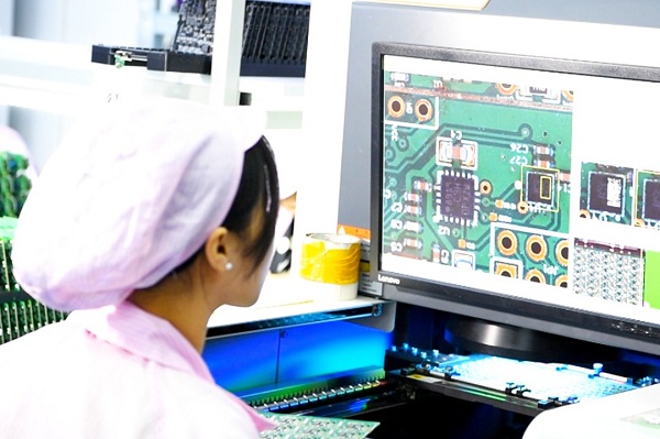
What Is Automated Optical Inspection (AOI)?Automated Optical Inspection, or AOI, is a technology used to visually inspect PCBs for defects during the manufacturing process. Unlike manual inspection, which relies on human eyes and is prone to errors, AOI uses high-resolution cameras and advanced software to scan and analyze the board. It identifies issues such as missing components, solder defects, and misalignments with incredible accuracy. AOI systems are typically integrated into various stages of PCB production, including bare board inspection, solder paste inspection, and post-reflow inspection. By automating the inspection process, manufacturers can achieve consistent results, even when dealing with complex designs or high-volume production.
Why Is AOI Needed in PCB Testing?Testing PCBs is a critical step in ensuring that electronic devices function as intended. Without proper testing, defective boards can lead to product failures, costly recalls, or even safety hazards. Here’s why AOI is a game-changer in PCB testing:
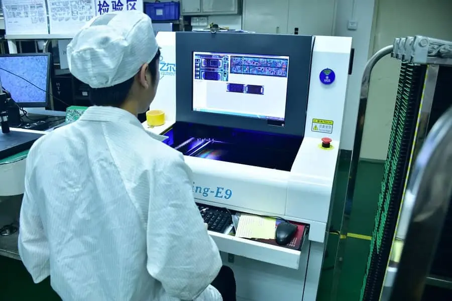
In PCB testing, AOI is often used after soldering to check for issues like solder bridges, insufficient solder, or misplaced components. By catching these problems early, manufacturers can avoid downstream issues that could compromise the final product.
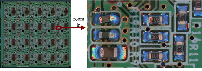
The Role of AOI in Solder Mask TestingSolder mask testing is a crucial aspect of PCB manufacturing. The solder mask is a protective layer applied to the board to prevent solder from bridging between conductive traces and to shield the board from environmental damage. Defects in the solder mask, such as pinholes, uneven coating, or misalignment, can lead to short circuits or corrosion over time. AOI plays a vital role in solder mask testing by providing a non-contact method to inspect the quality of the mask. Here’s how AOI contributes:
By integrating AOI into solder mask testing, manufacturers can ensure that the protective layer performs its role effectively, ultimately enhancing the durability and reliability of the PCB.
AOI and the Solder Mask Production MarketThe solder mask production market has seen significant growth in recent years, driven by the increasing demand for high-quality PCBs in industries like consumer electronics, automotive, and telecommunications. As PCBs become more complex, the need for precise solder mask application and inspection has never been greater. According to recent industry reports, the global market for automated inspection systems, including AOI, is projected to grow at a compound annual growth rate (CAGR) of over 13% from 2023 to 2030, reaching a value of approximately USD 72.9 billion by the end of the decade. This growth is closely tied to advancements in PCB manufacturing and the rising adoption of automation technologies. In the context of the solder mask production market, AOI systems are becoming indispensable for several reasons:
As the solder mask production market continues to evolve, manufacturers are increasingly relying on AOI to maintain a competitive edge. The technology not only improves product quality but also streamlines production processes, reducing waste and enhancing efficiency.
Benefits of AOI Beyond Defect DetectionWhile AOI is primarily known for its role in defect detection, its benefits extend far beyond that. Here are some additional advantages that make AOI a must-have in PCB manufacturing:
These benefits highlight why AOI is not just a tool for inspection but a strategic asset for manufacturers looking to stay ahead in a competitive industry.
Challenges of Implementing AOI and How to Overcome ThemDespite its many advantages, implementing AOI in PCB manufacturing is not without challenges. Understanding these hurdles and how to address them can help manufacturers make the most of this technology.
By addressing these challenges, manufacturers can fully harness the power of AOI to improve their production processes.
How AOI Enhances Overall Manufacturing EfficiencyIn addition to improving quality, AOI significantly enhances manufacturing efficiency. By automating the inspection process, it reduces the need for manual labor, which is often a bottleneck in production lines. This allows manufacturers to allocate human resources to other critical tasks, such as design optimization or customer support. Moreover, AOI minimizes the risk of defective products reaching the market. For example, catching a solder bridge defect during the post-reflow stage prevents the need for costly repairs or replacements later in the supply chain. This not only saves money but also protects the manufacturer’s reputation for reliability. Finally, AOI supports faster time-to-market. With quicker inspections and fewer delays caused by defects, manufacturers can meet tight deadlines without compromising on quality. In industries where speed is a competitive advantage, this can make a significant difference.
Future Trends: AOI and the Evolution of PCB ManufacturingAs technology continues to advance, AOI systems are evolving to meet the demands of next-generation PCB manufacturing. Here are some trends to watch:
These advancements suggest that AOI will remain a critical component of PCB manufacturing for years to come, adapting to the growing complexity of electronic devices.
Conclusion: The Indispensable Role of AOIAutomated Optical Inspection (AOI) is not just a luxury but a necessity in modern PCB manufacturing. From ensuring precision in PCB testing to enhancing solder mask quality and meeting the demands of the solder mask production market, AOI delivers unmatched accuracy, speed, and efficiency. Its ability to detect defects, reduce costs, and improve overall product reliability makes it an essential tool for manufacturers aiming to stay competitive. By integrating AOI into their production lines, manufacturers can achieve higher quality standards, streamline operations, and adapt to the evolving needs of the electronics industry. As technology continues to advance, AOI will only become more integral to the future of PCB manufacturing. Share · · · · The Role of Flux in PCB Wave Soldering: Selection, Application, and Residue RemovalMarch 16, 2026PCB wave soldering flux types include rosin, water-soluble, and no-clean options with varying activity levels for oxide removal and solder flow. This guide covers selection criteria, spray foam drop-jet application methods, residue removal processes, and alternatives like nitrogen blanketing to boost joint reliability and yields for engineers. Article Achieving Uniform Solder Fillets in PCB Wave Soldering: Process ControlMarch 16, 2026Achieve uniform solder fillets in PCB wave soldering with process control strategies. Optimize flux, preheat, wave height, conveyor speed for consistent fillet shape, height, and wetting balance. Includes visual inspection tips and troubleshooting for reliable through-hole assemblies. Boost quality in production. Article Optimizing Conveyor Speed for Efficient PCB Wave SolderingMarch 16, 2026Learn PCB wave soldering conveyor speed calculation to manage dwell time, immersion depth, and throughput effectively. Electric engineers get practical steps, best practices, and troubleshooting tips for higher process efficiency and fewer defects in wave soldering operations. Article Understanding IPC Standards for PCB Surface Finishes: Ensuring Quality and ComplianceMarch 11, 2026Understand IPC standards IPC 4552 ENIG and IPC 4553 immersion silver for PCB surface finishes. Ensure compliance, enhance solderability, and prevent common defects to achieve reliable, high quality circuit boards. Article Miniaturization Challenges in PCB AssemblyMarch 11, 2026Navigate the complexities of high density interconnect PCB assembly and precise component placement. Learn to tackle miniaturization challenges, from tiny part handling to thermal stress, ensuring robust and reliable electronics. Article High Speed Routing Techniques: PCBMarch 11, 2026Master high speed routing in PCBs to ensure signal integrity and minimize electromagnetic interference. Learn essential techniques for robust designs, from controlled impedance to differential pair strategies. Prevent performance issues and achieve reliable electronics. ArticleGet Instant PCB |